Blog post 2 #2
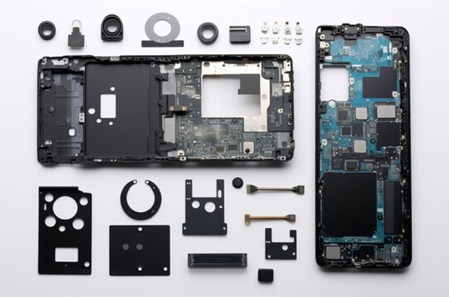
While the first interaction with an electronic device often remains limited to its external surface, casing, connectors, shell, and screen, the auditor cannot stop there. To truly understand how a device works, and therefore find exploitable vulnerabilities, you need to take it to the next level by accessing its inner workings. This is where things get serious, with two complementary steps: disassembly, to open the device and access the electronics, and characterization, to methodically map everything hidden on its circuit board.
These two phases form the foundation of any hardware pentest. If they’re poorly executed, the entire analysis can be compromised. But with precision, they pave the way for a deep understanding of the system and the discovery of the first weaknesses.
Disassembly: getting inside
The main objective of disassembly is to gain physical access to the circuit boards that make up the device, typically well protected inside a casing. In practice, however, this step requires a methodical approach and sometimes a degree of dexterity to avoid damaging the contents. Hidden screws, fragile clips, industrial adhesives, or welded shells; each model has its own set of challenges. For simpler products such as thermostats, IP cameras, or smart home devices, the process is often straightforward. But once you move on to more complex or highly miniaturized equipment, disassembly becomes a real technical challenge. Added to this is sometimes a legal or regulatory risk, especially with sensitive or proprietary hardware. And of course, any disassembly is destructive to varying degrees, it is always best to have multiple units available to avoid delaying the analysis.
Nonetheless, this effort is essential. Direct contact with the board is the sine qua non for identifying certain critical points, locating physical interfaces, and interacting with electronic components in the subsequent stages.

Characterization: making the board speak
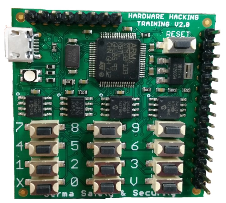
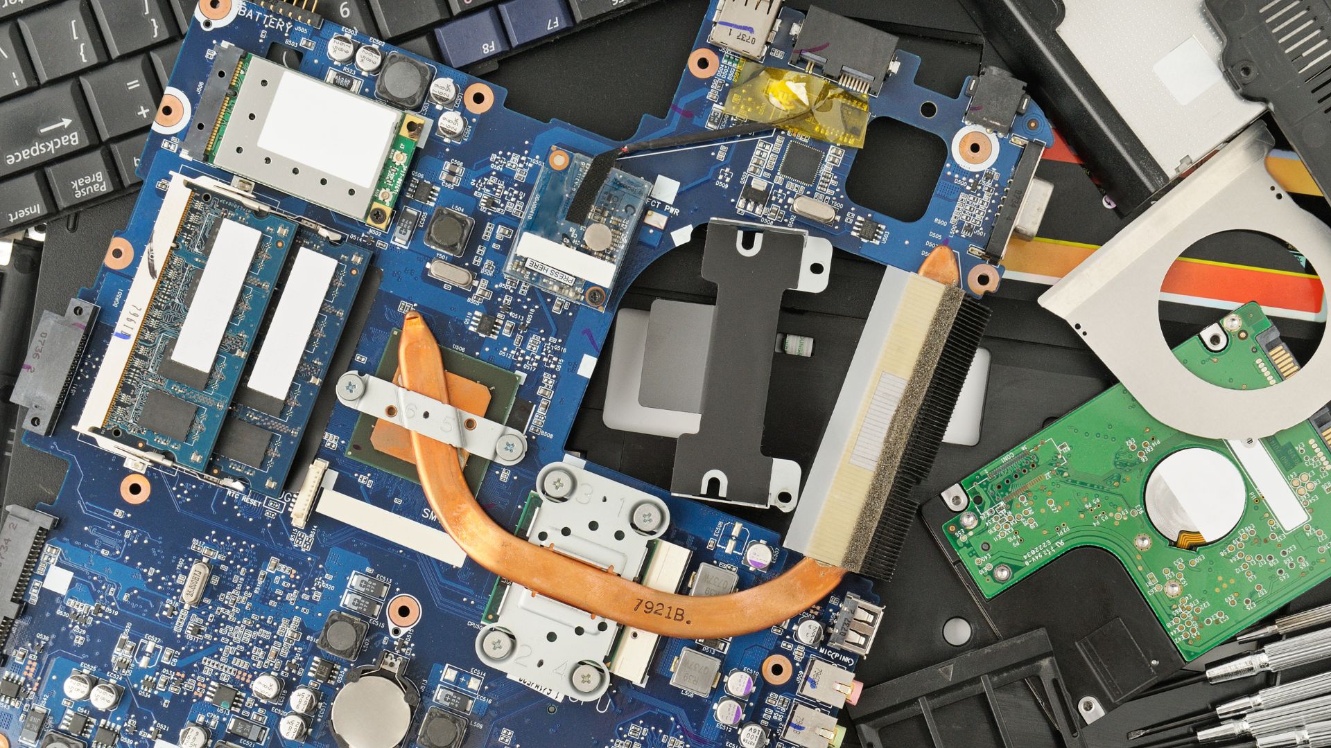
Once the PCB is exposed, the auditor enters a phase of meticulous observation: characterization. The goal is to understand, without yet interacting, how the board is designed and how it communicates. It all starts with visual inspection. The overall layout is examined, the most significant chips identified, visible connectors and pin groups located. The silkscreen, markings, and characteristic patterns (such as the typical alignment of UART pins or the cross arrangement of SPI traces) are carefully scrutinized. In some cases, a simple resistor placed between two pins can indicate an I2C bus.
This collection of clues also involves carefully reading the references on the chips present. Even partial markings or obscure inscriptions can lead to datasheets online. These documents are treasure troves of information: pinout, nominal voltage, supported protocols, operating modes…
At this stage, investigative tools come into play. A multimeter can identify ground (GND) or power (VCC) pins, which is essential to avoid errors during connections. A logic analyzer or oscilloscope is then used to observe actual signals on suspected lines: a UART burst at startup, cyclical I2C communication, SPI traffic to a Flash memory. We then begin to glimpse how the machine operates and, importantly, what means could be used to communicate with it.

And in all of this, how will Hardsploit NG make your life easier?
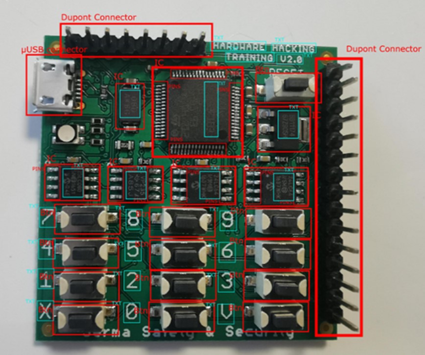
With Hardsploit NG, hardware characterization will enter the era of artificial intelligence. Whereas the identification of electronic components on a board until now relied on human experience and tedious visual and manual inspections, the new version will integrate artificial intelligence that will allow, through a simple photo of the PCB, to identify components, read the silkscreen, and instantly provide the corresponding datasheets for the components.
This advancement saves valuable time, avoids transcription or interpretation errors, and gives instant access to the documentation of identified circuits. The system leverages databases and deep learning models to link a component to its manufacturer references, even if the markings are partial or hard to read. The Hardsploit NG board, continuing its goal to position itself as the Swiss army knife of pentesting, will also include features such as a multimeter, logic analyzer, and oscilloscope.

In this way, Hardsploit NG makes characterization an intuitive, fast, and accessible step, even for those who are not electronics experts. The auditor can then focus on vulnerability research while leveraging reliable and comprehensive information about the entire board provided by Hardsploit NG.
What this teaches us
These first two steps are not simply about “looking at a board.” They are strategic. The quality of these steps will determine the rest of the audit: firmware recovery, interface exploitation, low-level debugging… And that’s exactly what we will cover in the next blog post!
Stay with us: Hardsploit NG has not yet finished revealing its secrets.
Protect your equipment with Hardsploit NG, our cutting‑edge hardware and IoT auditing solution.


